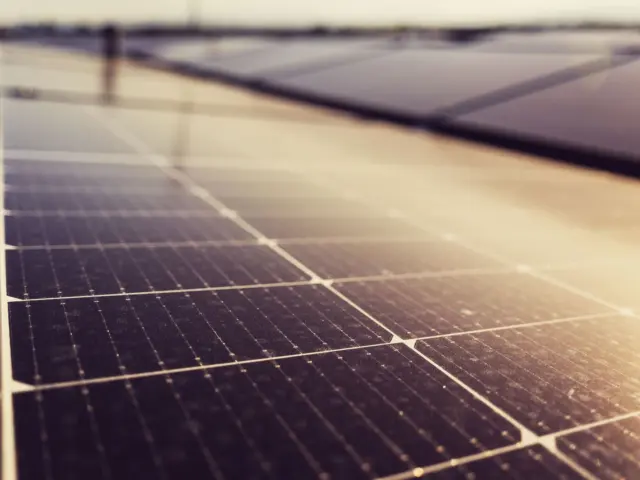
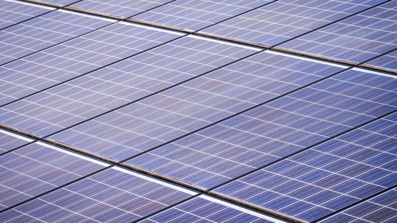
Thin film vs crystalline silicon solar panels is a choice between a thin semiconductor coating and a sliced silicon wafer. Crystalline silicon accounts for almost all production today, while thin film holds a small share built mainly on cadmium telluride and CIGS.
Thin-film cells also underpin the bendable, lightweight products described in the guide to flexible solar cells, which is the best starting point for the wider story of the technology.
Two ways to build a solar module
A solar module, the part most people call a solar panel, is made up of several small solar cells wired together inside a protective casing, as the U.S. Department of Energy (DOE) explains. What differs between the two families is the material that absorbs the light and how that material is put in place.
In a crystalline silicon module, the absorber is a wafer cut from a silicon ingot. In a thin-film module, a coating of a different semiconductor, such as cadmium telluride (CdTe) or copper indium gallium diselenide (CIGS), is deposited in a layer far thinner than a wafer. DOE notes that CdTe cells are called thin-film because they are more absorptive than other types of photovoltaics, such as silicon solar cells, and so require thinner layers to absorb the same amount of light.
Both families rely on the same photovoltaic effect, which the explainer on how do solar panels work covers from the start, so this article concentrates on the differences that matter when the two types are compared.
Crystalline silicon: the market default
Silicon wafer-based technology accounted for about 98% of total production in 2025, according to the Fraunhofer ISE Photovoltaics Report published in July 2026. The DOE reported that monocrystalline silicon represented 96% of global solar shipments in 2022, making it the most common absorber material in modules.
Making a silicon module is a sequence of mechanical and chemical steps. Mined quartz is purified into solar-grade silicon, cylindrical monocrystalline ingots are pulled from a vat of molten silicon, and diamond-wire saws slice the ingots into thin wafers that are processed into cells with anti-reflection coatings and electrical contacts. The same Fraunhofer report records how much that process has been squeezed: silicon usage fell from around 16 g/Wp in 2004 to about 2.0 g/Wp in 2024, thanks to higher efficiencies, thinner wafers and larger ingots.
The cell design itself keeps changing. According to the DOE, aluminum back surface field cells dominated the global market until approximately 2018, when passivated emitter rear contact (PERC) designs overtook them, and a further transition from PERC to n-type technologies such as heterojunction and tunnel-oxide passivated contact (TOPCon) cells is under way. Fraunhofer ISE adds that monocrystalline n-type TOPCon technology has become dominant, and its 2025 production table lists no multi-crystalline output. Newly produced modules are therefore almost all monocrystalline.
Reliability is the other pillar of silicon’s position. The DOE states that crystalline silicon cells reach module life spans of 25+ years and exhibit power degradation less than 1% a year. Silicon is also the second most abundant element in Earth’s crust after oxygen, so the raw material is not the constraint.
Thin film: layers instead of wafers
Thin-film modules build the light-absorbing layer directly on a supporting sheet. For CdTe, the DOE describes how CdTe vapor is deposited onto a coated conductive glass sheet, after which laser scribing and further deposition steps form the finished cell. The department also reports that CdTe is the second most common photovoltaic technology after crystalline silicon, representing 21% of the U.S. market and 4% of the global market in 2022.
The DOE lists several manufacturing points in CdTe’s favour. Cadmium and tellurium are byproducts of zinc and copper mining, a high-throughput line can produce a module in under 4.5 hours, and more than 90% of a module can be recycled once it is decommissioned. The department also states that CdTe module production requires six times less carbon dioxide than silicon.
CIGS is the second main thin-film chemistry. Per the DOE description of CIGS, it is a direct-bandgap material that can absorb a significant portion of the solar spectrum, enabling it to achieve the highest efficiency of any thin-film technology. A review in npj Flexible Electronics notes, however, that it has proved difficult for CIGS to reach double-digit market shares, and that only a handful of the many companies active in the field have survived the energy market.
A newer thin-film family is also advancing quickly in the laboratory. Fraunhofer ISE lists the record lab cell efficiency for perovskite solar cells at 26.9%, but those devices have their own durability questions, which the article on perovskite solar cells covers separately.
Efficiency and market share side by side
Efficiency decides how many square metres of panel a given output needs. Over the past decade, the efficiency of commercial silicon modules based on monocrystalline wafers has risen from about 17% to just under 25%, while the CdTe module efficiency increased from 15.6% to almost 20%, based on the July 2026 Fraunhofer ISE report. The same report gives a weighted average of 22.7% for crystalline silicon wafer-based modules in the fourth quarter of 2024.
| Measure | Crystalline silicon (wafer-based) | Thin film |
|---|---|---|
| Share of global production, 2025 | About 98% | Between 2 and 3 per cent |
| Record laboratory cell efficiency (2026 report) | 28.1% (monocrystalline) | 23.4% (CIGS); 21.0% (CdTe) |
| Commercial module efficiency | 22.7% weighted average, Q4-2024 | Almost 20% (CdTe) |
Table data: Fraunhofer ISE Photovoltaics Report, July 2026; the thin-film production share counts only one manufacturer, so it understates the whole thin-film sector.
Higher efficiency has a cost effect beyond space. The DOE notes that higher efficiencies reduce the cost of the final installation because fewer solar cells need to be manufactured and installed for a given output. On a limited area, a more efficient module delivers more power from the same footprint.
Weight, flexibility and special uses
Thin film earns its place where a rigid, framed silicon panel does not fit. The npj Flexible Electronics review reports CIGS record cells on flexible polyimide substrates, from 12.8% in 1999 up to a 21.38% cell in 2022, and 18% at laboratory scale on steel substrates. The DOE’s CdTe page also shows research on flexible CdTe solar cells on ultrathin glass.
The same review highlights flexible photovoltaics for terrestrial and extraterrestrial uses, noting that CIGS technology has consistently shown radiation tolerance and persistent performance under low-intensity, low-temperature conditions. Those traits explain the interest in thin film for vehicle-integrated and space-related uses.
Weighing the two for a given project
No single type wins on every measure, so the sensible comparison is by requirement:
- Available area: where space is tight, the higher module efficiency of crystalline silicon means fewer panels for the same output.
- Weight and shape: curved surfaces and light structures are where flexible thin-film products are being developed.
- Lifetime: silicon modules are documented at 25+ years with degradation under 1% a year, which is the benchmark for any competing type.
- Energy payback: a system in Sicily using wafer-based silicon modules has an energy payback time of about one year, and over a 20-year lifetime that type of system can produce twenty times the energy invested in it.
- End of life: Fraunhofer ISE says PV modules can be recycled, recovering rare and valuable materials, while the DOE puts CdTe recyclability above 90%.
Choosing a specific product, sizing a system and connecting it to a building are jobs for qualified local professionals, since conditions and rules differ by country.
Frequently asked questions
Can thin-film solar panels bend?
Some can. Flexible CIGS cells have been made on polyimide and steel substrates, and CdTe has been demonstrated on ultrathin glass. Standard thin-film modules built on a glass sheet are rigid.
Why is thin film such a small part of the market?
Fraunhofer ISE puts thin film at a few per cent of production, and the CIGS review points to the difficulty of competing in an energy market where silicon is well understood and its manufacturing is highly optimized.
Is multicrystalline silicon still made?
Fraunhofer ISE’s 2025 production breakdown shows monocrystalline silicon and thin film only, with no multicrystalline output, so new modules are almost entirely monocrystalline.
Can solar modules be recycled?
Yes. Fraunhofer ISE states that PV modules can be recycled and recovered materials reused, although more research is needed to make recycling cheaper and more thorough.