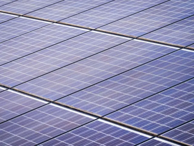
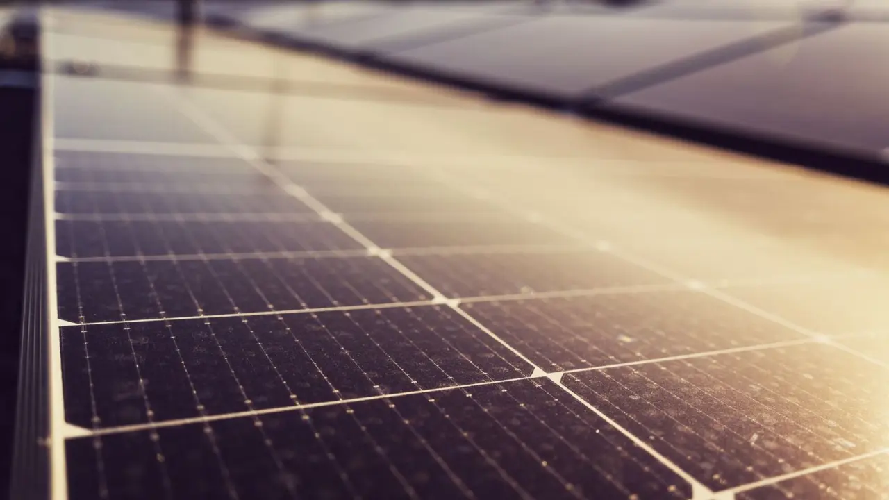
Gallium arsenide solar cells are photovoltaic cells built from a compound of gallium and arsenic rather than silicon. Made as an extremely thin film and lifted off a reusable wafer, they hold efficiency records but remain costly to produce.
This page is part of the guide to flexible solar cells, and it explains the technology that Alta Devices developed. It is an independent explainer and is not affiliated with Alta Devices, Hanergy or any other maker.
How gallium arsenide turns sunlight into electricity
Every solar cell works the same way at its core: a photon with enough energy knocks an electron out of a filled energy band into an empty one, and the cell collects that electron as current. The energy gap between the two bands is called the band gap. Gallium arsenide, usually shortened to GaAs, is a compound semiconductor with a band gap of 1.4 eV, according to a Lawrence Berkeley National Laboratory article that describes stacking it under a layer of gallium indium phosphide with a band gap of 1.8 eV.
What sets GaAs apart is how it handles the energy of an excited electron. If an electron is not pulled out of the cell fast enough, it decays and gives up its energy as heat or as light. A 2011 report in MIT Technology Review explained that in gallium arsenide almost all of the electrons produce light rather than heat, and that in the highest-quality material the cycle of light production and reabsorption can happen 100 times per incoming photon. Each reabsorbed photon gives the cell another chance to produce current, which is why Caltech professor Harry Atwater called the material “almost an ideal solar-cell material” in that article.
Epitaxial lift-off: how the thin film is made
The word epitaxy means growing a crystal layer on top of another crystal so that the new layer copies its atomic pattern. To make a GaAs cell, manufacturers grow the light-absorbing layers on a high-quality GaAs wafer. In the version of the method that Alta Devices used, the Technology Review report said the wafer serves as a template for very thin crystalline layers; the layers are then freed from the wafer with chemical etching and lifted off, which allows the wafer to be used again. The article added that an early version of the technique was pioneered by Alta Devices cofounder Eli Yablonovitch in the 1980s.
The result is a film rather than a wafer. Semiconductor Today described the company as fabricating GaAs cells in a micron-thick thin film that it then lifted off the growth substrate, with the substrate reused multiple times to amortize its high cost, and the finished thin-film cell could be placed on a flexible backing. In 2019, pv magazine USA reported the same process as producing flexible layers of GaAs measuring 1 micron thick. A micron is a thousandth of a millimetre, so the active layer is thin enough to bend with whatever it is attached to.
Researchers kept refining the lift-off step after the first commercial attempts. A paper published on 12 March 2013 in Nature Communications noted that conventional epitaxial lift-off requires several post-processing steps to restore the substrate to an epi-ready condition, and presented a scheme that minimizes post-etching residues and keeps the surface smooth, leading to direct reuse of the gallium arsenide substrate. The same paper showed full-wafer GaAs thin-film transfer onto both rigid and flexible substrates.
Efficiency records and the theoretical limit
Efficiency is the share of incoming sunlight that a cell converts to electricity. For a cell with a single junction, there is a ceiling. The 2011 Technology Review report said Alta Devices had achieved a record solar-cell efficiency of 28.2 percent, nearing the theoretical maximum of 33.5 percent. The same report cautioned that the record cells were small, one-off devices and that the company’s larger solar modules were at about 21 percent, because efficiency typically drops when production scales up.
Later results were certified by an outside laboratory. According to Semiconductor Today in 2014, Alta Devices’ single-junction and dual-junction cells reached 28.8 percent and 30.8 percent respectively, as certified by the US National Renewable Energy Laboratory (NREL). In July 2018, the same publication reported that NREL had certified an increase of the single-junction record to 28.9 percent, and that Alta had set the GaAs single-junction record five times since 2010.
| Year reported | Device | Efficiency | Status |
|---|---|---|---|
| 2014 | Single-junction GaAs cell | 28.8% | Certified by NREL |
| 2014 | Dual-junction cell | 30.8% | Certified by NREL |
| 2018 (July) | Single-junction GaAs cell | 28.9% | Certified by NREL |
The figures in this table come from Semiconductor Today’s 2014 report and its 2018 report.
Stacking several junctions goes further. By depositing gallium indium phosphide on gallium arsenide, NREL investigators created a tandem cell with a proven 30-percent efficiency, as the Berkeley Lab article recounted in 1999. More recently the NLR photovoltaic research page reported that in 2015 its researchers demonstrated about 46% efficiency with a four-junction inverted metamorphic cell, and later 47.1% efficiency at 143 suns with a six-junction version. Those results use concentrated sunlight, and the devices contain more than 100 independent layers, so they are not directly comparable with a flat single-junction cell in ordinary sunlight.
Why gallium arsenide cells cost so much
The NLR photovoltaic group states that the cost of III-V devices is very high at present, which limits their use to high-concentration and space applications, according to its low-cost III-V research page. The group names the two major costs as the epitaxy, meaning the growth of the crystal layers, and the single-crystal substrates used for growth. Those substrates are typically a perfect single crystal of GaAs or germanium, and both are described as too expensive to enable widespread terrestrial use of III-V solar cells.
The same page describes work on cutting both costs. Its hydride vapor-phase epitaxy approach uses low-cost elemental source materials and has demonstrated high-quality growth at rates that could make a high-efficiency solar cell in less than a minute, compared with the hours it takes today. The group reported single-junction GaAs cells with more than 25% conversion efficiency grown at rates exceeding 5 micron per minute. In 2011, Technology Review noted that the growth method then used, chemical vapor deposition, was too slow to make cheap cells, which is the same bottleneck.
Lift-off addresses the second cost, since a wafer that can be reused spreads its price over many cells. It does not remove the first cost, because each new film still has to be grown layer by layer on the wafer.
Where thin-film gallium arsenide cells are used
Space is the established market. The NLR research page says III-V multijunction solar cells power the majority of satellites, and a 2012 Technology Review profile noted that GaAs had been used in solar cells on satellites and spacecraft for decades.
The flexible film opened a second market built on weight. The 2019 pv magazine USA report said Alta was gaining customers in the UAV and space industry such as Boeing and AeroVironment. Small aircraft are limited by the area they can cover with cells, which makes the output per square metre decisive, and the page on solar powered drones follows that application in more detail.
When Hanergy completed its purchase, Semiconductor Today reported that it planned to expand the application of Alta’s products in mobile power, ranging from emergency charging of mobile phones to the automotive sector and the Internet of Things. The next section covers what became of the company.
The history of Alta Devices’ gallium arsenide cells
Alta Devices was founded in 2007 and based in Santa Clara, California, as Technology Review reported in 2011. It raised more than $120 million from investors including Kleiner Perkins Caufield and Byers and Dow Chemical, pv magazine USA reported, before Hanergy, a Beijing-based clean-energy group, completed its acquisition on 14 August 2014, according to Semiconductor Today. On 3 July 2018, Semiconductor Today reported that NREL had certified the company’s 28.9 percent record, set under Hanergy’s ownership. On 19 December 2018, Semiconductor Today reported a further single-junction GaAs record of 29.1 percent, certified by the CalLab at Fraunhofer ISE.
The company then ran out of backing. In December 2019, pv magazine USA reported that Alta Devices had furloughed almost all of its Sunnyvale, California staff without pay or notice, affecting almost 250 employees, and quoted a source who said Hanergy had stopped funding the company. In November 2020, pv magazine USA reported that an auction put the physical and intellectual property remains of the company on the block.
The technology did not fail on performance. The records stood, and the 2011 Technology Review report had already flagged the open question: Alta needed to show that its high-efficiency cells would last for decades in the weather without a significant loss of performance. For how output declines in any panel over time, the page on solar panel lifespan explains the usual pattern.
Frequently asked questions
What are gallium arsenide solar cells made of?
They are made of gallium arsenide, a compound of the elements gallium and arsenic, usually grown as thin crystalline layers. Multijunction versions add layers of other compounds, such as gallium indium phosphide, to capture more of the spectrum.
What is epitaxial lift-off?
Epitaxial lift-off is a process in which thin crystal layers grown on a GaAs wafer are separated from it by chemical etching so that the wafer can be reused. The lifted film can then be attached to a flexible backing.
How efficient are gallium arsenide solar cells?
The last single-junction GaAs record Alta Devices reported, in December 2018, was 29.1 percent, according to Semiconductor Today, and multijunction III-V cells have reached higher figures under concentrated sunlight. Complete modules convert less than the best small cells.
Why are gallium arsenide solar cells not common on homes?
According to the NLR research page, the cost of III-V devices limits their use to high-concentration and space applications. The crystal substrates and the slow growth process drive that cost.